Seyed Masoud Hosseini · Overview · Study log · Weekly summaries · Ideas · Search · Transcript · RSS feed
Circuits & Electronics · Lecture 15 of 26 · 48:00
Lecture 14: State and Memory Using Capacitors
Study guide
What this lecture covers
Taught by a recitation instructor filling in, this lecture pivots from RC transient analysis to its use in digital memory. It reviews the general RC step response, formalizes the idea of "state" as the information a capacitor carries about the past, and decomposes any RC response into a zero state response (ZSR) and a zero input response (ZIR). It then builds a minimal memory cell from a switch and capacitor, shows that replacing the switch with a MOSFET gives essentially a DRAM cell, and progressively improves the design with a buffer (to slow the leak) and feedback (to make it hold state indefinitely, turning it into static memory).
After watching, you can explain what "state" means for a capacitor, decompose an RC response into ZSR and ZIR, describe why a DRAM cell must be periodically refreshed, and explain how adding an isolating buffer and a feedback path converts a leaky, disturbance-prone memory cell into a robust static memory cell.
Key ideas
- State: the summary of all past inputs relevant to predicting a circuit's future behavior; for a linear capacitor, either charge
qor voltagevcserves as the state variable, sinceq = Cv. - General RC step response:
vc(t) = VI + (vc(0) - VI) e^{-t/RC}, combining an initial valuevc(0)and a final valueVI. - Zero state response (ZSR): the response to an input with the capacitor's initial state set to zero.
- Zero input response (ZIR): the response of the initial state decaying to equilibrium with no input applied (
vI = 0). - Superposition of ZSR and ZIR: the full response is the sum
vc = vc,ZSR + vc,ZIR, a technique useful for arbitrary (not just step) inputs. - Basic memory element: a switch (or MOSFET) connecting an input to a storage capacitor; closing the switch samples the input voltage onto the capacitor, and the stored charge persists (temporarily) after the switch opens.
- DRAM cell: replaces the ideal switch with a MOSFET acting as a controlled resistor/open-circuit; the stored charge decays over time (
vc = VOH * e^{-t/RC}), requiring periodic refresh — hence "dynamic." - Buffering and feedback: an isolating buffer (high input resistance) slows the capacitor's discharge, extending valid storage time; a feedback path from output back to input turns the leaky cell into a static memory that holds its value as long as the circuit is powered.
Walkthrough
Review of the RC step response and its implicit assumption (5:20)
The lecture restates the general solution vc(t) = VI + (vc(0) - VI)e^{-t/RC} for a step input applied at t=0, and points out an implicit assumption behind this: the circuit must contain some switch that establishes the input value exactly at t=0, since the response depends only on the initial capacitor voltage and the input from that point forward, not on the input's earlier history.
Defining "state" (7:45)
The lecture defines the state of the capacitor as the summary of all past information needed to predict its future response, and notes that while the physically stored quantity is charge q = Cv, for a linear capacitor the voltage v is an equally valid state variable since the two are proportional.
Decomposing the response: ZSR and ZIR (11:35)
The lecture separates the general response into two special cases: the zero state response (starting from zero charge, responding only to the input, vC,ZSR = VI(1 - e^{-t/RC})) and the zero input response (starting from an initial charge with no input applied, vC,ZIR = vc(0)e^{-t/RC}). The full response is their sum, a superposition result that generalizes beyond step inputs to ramps, impulses, or more complex waveforms.
Why computing needs memory (18:40)
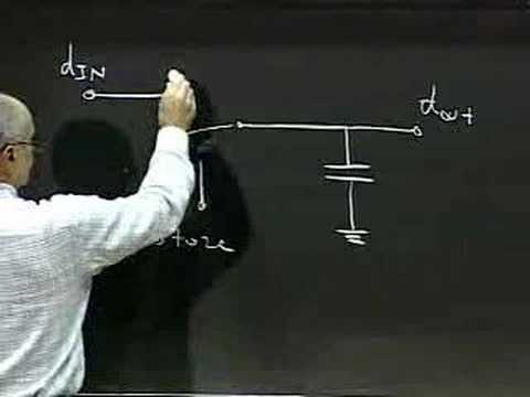
The lecture motivates memory by noting that many computations (such as a running sum) depend on previous results, so a complete computing system needs both combinational logic and memory to store intermediate results. It defines the basic memory abstraction: a block with a store control input, a dIN input, and a dOUT output that holds whatever value was present on dIN at the moment store was asserted, and should otherwise remain undisturbed.
Building the cell: switch, capacitor, and the MOSFET version (23:25)
The lecture implements the memory abstraction directly: a switch connects dIN to a storage capacitor; closing and reopening the switch leaves the capacitor holding whatever voltage was present on dIN. Replacing the ideal switch with a MOSFET (acting as a resistor when the gate is high and an open circuit when the gate is below threshold) gives essentially the basic cell used in a DRAM. The lecture works through the resulting decay: once the switch opens, the capacitor's voltage decays as vc = VOH*e^{-t/RC}, and the cell only stores a valid logical one for as long as this stays above the output-high threshold — the reason DRAM must be periodically refreshed.
Extending storage time with a buffer (32:45)
To reduce loading on the storage node, the lecture adds a buffer (such as an inverter or source follower) with high input resistance between the capacitor and the next stage. Because the relevant discharge time constant is now set by this much larger input resistance rather than the small load resistance, the valid storage time increases substantially. Typical DRAM numbers are given: input resistances around a gigaohm and storage capacitances of roughly a femtofarad to a picofarad, giving time constants from about a microsecond to a millisecond — explaining why real DRAM needs refresh cycles on the order of milliseconds.
From leaky memory to static memory with feedback (40:05)
A live demo shows the storage capacitor discharging within about a second once a resistive load is present, losing its stored state. Adding a feedback switch that routes the buffered output back to the input (active only when not actively storing) keeps refreshing the capacitor automatically, producing a static memory that holds its value indefinitely as long as the circuit is powered. The demo also shows a remaining flaw: without isolation, disturbing the output node directly can flip the stored state, which the lecture fixes by buffering the output before feeding it back, so external disturbances no longer propagate into the storage node.
Assembling a small memory array (45:01)
In the final minutes, the lecture shows a four-bit memory built from four of these cells, each gated by an AND operation with a decoder output. The decoder's truth table ensures that for a given binary address, only one AND gate output is high, so only the addressed cell samples the input when store is asserted — the basic addressing scheme scaled up to build much larger memory systems.
Before you watch
- Review the RC step-response derivation and the "Practice it Like Perreault" intuitive sketching method from the previous lecture (Lec 13).
- Be comfortable with the MOSFET's on/off (SR) behavior used to model it as a switch.
- Recall basic digital logic elements (inverters, AND gates) from earlier in the course.
Check your understanding
- What is the "implicit statement" the lecture points out about the standard RC step-response equation, and why does it matter?
- How do the zero state response and zero input response combine to give the full response of an RC circuit, and why is this decomposition useful for non-step inputs?
- Why must a DRAM cell built from a MOSFET and capacitor be periodically refreshed?
- How does adding a high-input-resistance buffer extend a memory cell's valid storage time?
- What problem does feeding the buffered output back to the storage node solve, and why is a second buffering stage needed to prevent external disturbances from corrupting the stored state?
Vocabulary
- state (noun)
- The stored information a system carries that summarizes its past.
The capacitor's voltage represents the circuit's state. - zero state response (noun)
- The output of a system when it starts with no stored energy and only reacts to the input.
The zero state response builds up from zero as the input is applied. - zero input response (noun)
- The output of a system decaying naturally from its starting state with no input applied.
The zero input response shows the stored charge dying away. - decompose (verb)
- To split a whole response into simpler separate pieces.
The full response can be decomposed into ZSR and ZIR. - memory cell (noun)
- A small circuit that can store one value until it is read or changed.
A switch and a capacitor together form a simple memory cell. - DRAM (noun)
- A common type of computer memory that stores each bit as charge on a tiny capacitor.
DRAM must be refreshed often because its charge leaks away. - decay (verb)
- To gradually reduce toward zero over time.
The stored voltage will decay unless it is refreshed. - refresh (verb)
- To restore a stored value before it is lost.
DRAM cells must be refreshed thousands of times per second. - buffer (noun)
- A circuit stage that isolates one part of a circuit from loading another.
Adding a buffer slows the leak from the storage node. - feedback (noun)
- Sending a system's output back into its own input.
Feedback lets the memory cell refresh itself automatically. - isolate (verb)
- To keep one part of a system separate so it is not affected by another part.
A second buffer isolates the storage node from outside disturbances. - decoder (noun)
- A circuit that turns a binary address into a signal that selects exactly one output.
The decoder picks which memory cell gets written. - recitation (noun)
- A smaller class session, often led by a teaching assistant, that reviews and applies lecture material.
A recitation instructor teaches this particular lecture. - implicit (adjective)
- Understood without being directly stated.
There is an implicit assumption behind the standard step response. - abstraction (noun)
- A simplified way of describing something that hides unneeded detail.
The store and dOUT ports define the memory abstraction. - address (memory) (verb)
- To select a specific location in memory using a code.
The decoder is used to address one memory cell at a time. - disturbance (noun)
- An unwanted change that disrupts normal operation.
External disturbances could flip the stored state without buffering. - sample (a value) (verb)
- To capture and store a value at a specific instant.
Closing the switch samples the input voltage onto the capacitor. - undisturbed (adjective)
- Not changed or affected by anything outside.
The stored value should stay undisturbed until read again. - running sum (noun)
- A total that keeps adding new values as they arrive.
Computing a running sum requires memory of previous results.
Chapters
- 0:00 Introduction
- 5:20 Implicit Statement
- 7:45 State
- 11:35 Zero State Response
- 18:40 Memory
- 23:25 Store
- 25:40 MOSFET
- 32:45 Buffer
- 36:27 Static RAM
- 40:05 Complement
- 45:01 Memory Example
From the YouTube description
State and memory
View the complete course: http://ocw.mit.edu/6-002S07
License: Creative Commons BY-NC-SA
More information at http://ocw.mit.edu/terms
More courses at http://ocw.mit.edu
← Lecture 13: Digital Circuit Speed and RC Delay · Lecture 15: Second-Order Systems - Deriving the LC Circuit Response →