Seyed Masoud Hosseini · Overview · Study log · Weekly summaries · Ideas · Search · Transcript · RSS feed
FPGA & Verilog Design · Lecture 12 of 12 · 23:46
Part 12: RISC-V Custom Peripheral
Study guide
What this lecture covers
Building on the RISC-V soft core from Part 11, this lecture answers how to add your own hardware peripheral to that processor. It explains FemtoRV's memory addressing scheme (RAM, I/O, and SPI flash pages using one-hot encoding for peripherals), then designs, simulates, and integrates a simple pulse-width modulation (PWM) driver that controls an LED's brightness from software.
By the end you can explain how a write to a specific address reaches a hardware driver through strobe and select signals, design and simulate a small peripheral module before wiring it into the system-on-a-chip, and write C code that writes to a memory-mapped address to control custom hardware. This is the final lecture in the introductory FPGA series.
Key ideas
- FemtoRV memory map: the top two address bits (22-23) select a page -
00for block RAM,01for memory-mapped I/O peripherals,10for SPI flash where program instructions live. - One-hot peripheral addressing: within the I/O page, only one bit is high at a time to select a given peripheral, trading available address space for simpler, cheaper driver hardware that only needs to check a single bit.
- Strobe and select signals: a peripheral only registers incoming write data when both a write-strobe line (asserted for one cycle on any I/O write) and its own select line (asserted when its specific address bit is targeted) are high.
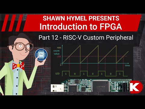
- PWM peripheral design: a free-running counter (0 to 4095 for 12 bits) is compared against a duty-cycle value written from software; the LED is on while the counter is below that value and off otherwise, producing a controllable average brightness.
- Registered initial values: setting a register's starting value directly in the Verilog declaration (supported by Yosys/iCE40) avoids needing an explicit reset line for this driver.
- Peripheral integration steps: define an address bit in the hardware config file, include the driver's source, instantiate it conditionally in the SOC top-level file, and connect it to shared strobe/data lines - while making sure it doesn't conflict with peripherals that already use the same output pins.
Walkthrough
Memory addressing in FemtoRV (0:25)
The lecture details the 32-bit addressing scheme: page bits select RAM, I/O, or SPI flash, and I/O addresses use one-hot encoding, illustrated with the LED driver's known address (0x400004). It shows how a peripheral's address is built in C as a base address plus a left-shifted bit position, and locates the hardware_config_bits.v file that lists which of FemtoRV's peripheral slots are free for a custom driver.
Designing the PWM hardware (5:18)
The PWM module declares a parameterized bit-width counter, a clock input, and write-strobe/select inputs. On each clock cycle, if both strobe and select are high, it latches the incoming write data into an internal duty-cycle register and resets the counter; otherwise the counter free-runs and wraps. The LED output is driven high while the counter is below the stored duty-cycle value.
Simulating the PWM driver (9:04)
A test bench (using a smaller 4-bit counter to keep the simulation short) writes several duty-cycle values - 0%, roughly 33%, and the maximum - and GTKWave confirms the LED output stays low, toggles at the expected point in the count, and can't quite reach a fully-on state with this simple scheme, which the lecture accepts as an acceptable simplification.
Integrating the peripheral into the SOC (12:15)
The PWM Verilog file is copied into FemtoRV's devices directory, a new address bit is defined in the hardware config file, the driver is included and conditionally instantiated in the SOC top-level Verilog (guarded by an ` ifdef ``), and its clock, strobe, select, and data lines are wired to the shared I/O bus signals - following the pattern used by other existing peripherals in the file.
Resolving the LED conflict and building (17:42)
Because the PWM driver and the plain LED driver from Part 11 both use the same output pins, the board config disables the LED driver's definition and enables the PWM one instead. Running make icestick synthesizes, places and routes, and uploads the updated SOC to the iCEstick.
Writing and testing the C program (19:49)
A new C program loops from 0 to 4095, writing each value to the PWM peripheral's memory address (computed manually as base address plus the peripheral's bit position) with a short delay between writes, producing a slowly brightening LED that resets to off - a software-controlled sawtooth brightness ramp - compiled and uploaded with make main.prog.
Before you watch
- Complete Part 11 ("RISC-V Softcore Processor"); this lecture directly extends that FemtoRV build and assumes the toolchain and board setup from it are already working.
- Recall the test bench and GTKWave workflow from Part 7, since the PWM driver is verified in simulation before touching hardware.
Check your understanding
- What do the page bits in FemtoRV's memory address determine, and what are the three possible destinations?
- Why does one-hot encoding for I/O addressing save logic cells, and what is the trade-off?
- What two conditions must both be true for the PWM driver to latch new write data?
- Why can't the LED driver and the PWM driver be enabled at the same time in this design?
- How does the PWM counter and comparison logic translate a single written value into a visible change in LED brightness?
Vocabulary
- memory map (noun)
- A layout showing which address ranges correspond to which parts of a system.
The memory map assigns separate pages for RAM, I/O, and flash. - one-hot encoding (noun)
- A coding scheme where exactly one bit is set to 1 to represent a choice.
Peripheral selection uses one-hot encoding within the I/O address page. - strobe signal (noun)
- A brief pulse signal indicating that data is ready to be used.
A write-strobe pulse tells the peripheral new data has arrived. - select signal (noun)
- A signal that identifies which specific device or unit should respond to a request.
The peripheral only reacts when its select signal is high. - duty cycle (noun)
- The proportion of time a signal stays on during one full cycle.
A higher duty cycle makes the LED appear brighter. - pulse-width modulation (PWM) (noun)
- A technique controlling average power by switching a signal on and off at varying proportions.
PWM controls the LED's brightness from software. - free-running (adjective)
- Describes a counter or process that keeps running continuously without external control.
The counter is free-running, wrapping around once it hits its maximum. - latch (verb)
- To store an incoming value into a register at a specific moment.
The driver latches the new duty-cycle value when strobe and select are both high. - conflict (noun)
- A situation where two components try to use the same resource incompatibly.
The LED driver and PWM driver have a pin conflict. - sawtooth (adjective)
- Describes a signal that rises steadily then drops sharply back to its start, repeating.
The program produces a sawtooth brightness ramp on the LED. - soft core (noun)
- A processor built from an FPGA's own logic instead of a fixed, dedicated chip.
FemtoRV is a RISC-V soft core added to the design. - address bus (noun)
- The set of wires that carries the location a processor wants to read or write.
The top two bits of the address bus select which memory page is used. - page (noun)
- A separate range of memory addresses set aside for one purpose.
The I/O page holds the addresses for all the peripherals. - assert (verb)
- To make a signal active, usually by setting it high.
The write-strobe line is asserted for one cycle on every I/O write. - offset (noun)
- A fixed amount added to a base value to reach a specific location.
The peripheral's address is the base address plus its bit offset. - counter (noun)
- A circuit that increases its stored value by a fixed amount on every clock cycle.
A free-running counter drives the PWM comparison. - comparator (noun)
- A circuit that checks whether one value is greater than, less than, or equal to another.
A comparator checks the counter against the duty-cycle value. - parameterize (verb)
- To make a design's size or setting adjustable instead of fixed.
The PWM module's counter width is parameterized. - reset line (noun)
- A signal used to force a circuit back to a known starting state.
Setting an initial value in the declaration removes the need for a reset line. - guard (verb)
- To protect a piece of code so it only runs under a certain condition.
An ifdef guards the driver so it only compiles in when needed. - conditional (adjective)
- Happening only when a certain condition is true.
The peripheral is instantiated conditionally in the SOC top-level file. - wire up (phrasal verb)
- To connect components together with signal lines.
The driver's clock and data lines are wired up to the shared bus. - delay function (noun)
- A piece of code that pauses a program for a set amount of time.
A delay function slows the brightness ramp so it is visible. - loop (verb)
- To repeat a set of instructions again and again.
The program loops from 0 to 4095, writing each value in turn. - manually (adverb)
- By hand, without an automatic tool doing the work.
The peripheral's address is computed manually in the C code. - extend (verb)
- To build further on something that already exists.
This lecture extends the FemtoRV soft core built in the previous part. - roughly (adverb)
- Approximately, not exactly.
One test writes a duty cycle of roughly 33 percent. - simplification (noun)
- A change that makes something easier by leaving out small details.
Not reaching a fully-on LED state is accepted as an acceptable simplification.
Chapters
- 0:00 Introduction
- 0:25 Memory Addressing
- 5:18 Hardware PWM Code
- 9:04 PWM Simulation
- 12:15 Implementation
- 17:42 Configuration
- 22:35 Outro
From the YouTube description
A field-programmable gate array (FPGA) is an integrated circuit (IC) that lets you implement custom digital circuits. You can use an FPGA to create optimized digital logic for things like digital signal processing (DSP), machine learning, and cryptocurrency mining. Because of the FPGA’s flexibility, you can often implement entire processors using its digital logic. You can find FPGAs in consumer electronics, satellites, and in servers used to perform specialized calculations.
In this series, we will see how an FPGA works and demonstrate how to create custom digital logic using the Verilog hardware description language (HDL).
Previously, we saw how to build an existing RISC-V softcore processor for the iCEstick and write a C test program for it. This time, we design a custom pulse-width modulation (PWM) hardware peripheral with Verilog and integrate it into the FemtoRV processor.
Note: you will need Linux to follow along! I did everything on a Raspberry Pi 4, but any Debian-based flavor (e.g. Ubuntu) should work.
The steps in this video can be found in written form here: https://www.digikey.com/en/maker/projects/introduction-to-fpga-part-12-risc-v-custom-peripheral/148dba8ecafe49a1ac7e13641088af4c
All code examples and solutions for this series can be found here: https://github.com/ShawnHymel/introduction-to-fpga
Bruno Levy’s learn-fpga FemtoRV repository: https://github.com/BrunoLevy/learn-fpga
RISC-V is an open source instruction set architecture (ISA) that can be used to design processors without paying a licensing fee. As a result, it is a great way to implement a softcore processor in an FPGA to learn about how CPUs work.
Building on what we learned last time, we will use our Verilog skills to design a custom PWM peripheral for the system-on-a-chip (SOC). The peripheral will contain a PWM register that can be written to from the CPU via code. A counter in the peripheral continuously counts up. Whenever the counter value is less than the value in the PWM register, the associated pin (e.g. LED) will be on. Whenever the value is greater than or equal to the PWM register, the pin will be off. With a fast enough clock speed, this should produce a dimmable LED that is constant to our eyes.
To control the PWM register, we must access it through a particular memory address in code. Two bits in the memory address space for the FemtoRV control the memory “page.” One page allows access to RAM (implemented in block RAM). Another page gives access to the “I/O” peripherals that control things like LEDs, buttons, OLED driver, etc. In our case, we will use the I/O bus to control the PWM peripheral. The final page gives access to program memory (allocated on the SPI flash chip).
While there is no challenge for this episode, you are encouraged to try making a peripheral of your own design and integrate it into the FemtoRV. Let us know in the comments or on Twitter (@DigiKey, @MakerIO, @ShawnHymel, @BrunoLevy01, #FemtoRV) if you make something cool!
Product Links:
https://www.digikey.com/en/products/detail/lattice-semiconductor-corporation/ICE40HX1K-STICK-EVN/4289604
Related Videos:
https://www.youtube.com/watch?v=z8Oldd-nrfs
https://www.youtube.com/watch?v=5kNXX67mchE
https://www.youtube.com/watch?v=iwcxLQ6AB88
Related Project Links:
https://www.digikey.com/en/maker/projects/introduction-to-fpga-part-12-risc-v-custom-peripheral/148dba8ecafe49a1ac7e13641088af4c
Related Articles:
https://www.digikey.com/en/pdf/r/renesas-electronics-america/powering-fpga-applications
https://www.digikey.com/en/videos/d/dsp/edge-machine-deep-learning-on-fpga
Learn more:
Maker.io - https://www.digikey.com/en/maker
Digi-Key’s Blog – TheCircuit https://www.digikey.com/en/blog
Connect with Digi-Key on Facebook https://www.facebook.com/digikey.electronics/
And follow us on Twitter https://twitter.com/digikey